It seems you're coming from the US.
Would you like to switch to the American website?
Micro-Epsilon America
No, stay on the Micro-Epsilon International Website
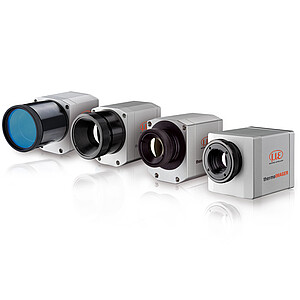
Measurement tasks in the semiconductor industry require highest accuracy and repeatability. Micro-Epsilon offers the right solution for numerous applications from precise machine positioning and wafer inspection to topographic measurements.
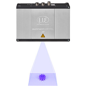
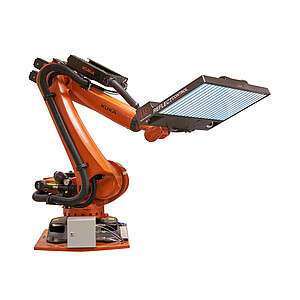
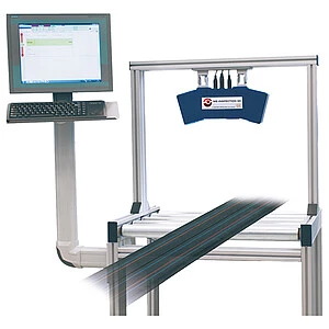
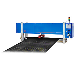
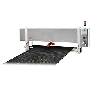
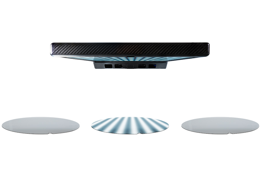
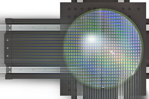
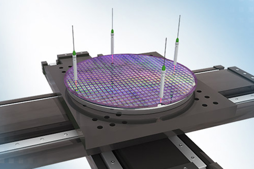
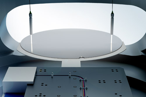
reflectCONTROL deflectometry systems are used to detect the flatness or planarity of 150 mm wafers. These measure the flatness with only one image. For this purpose, the sensors project a striped pattern onto the wafer, which is recorded by the…
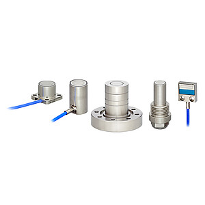
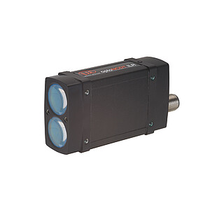
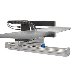
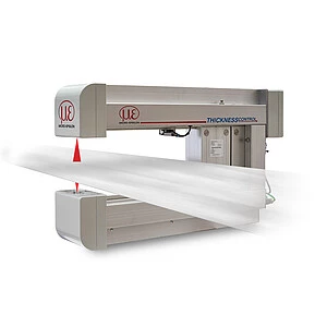
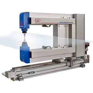
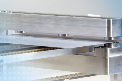
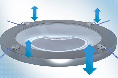
Capacitive displacement sensors are used for the exact thickness measurement of wafers. Two opposing sensors detect the thickness and also determine other parameters such as deflection or sawing marks. The position of the wafer in the measuring…
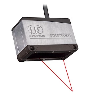
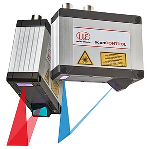
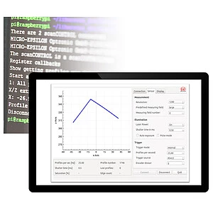
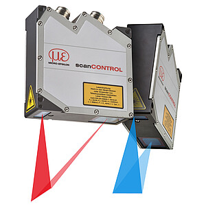
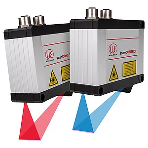
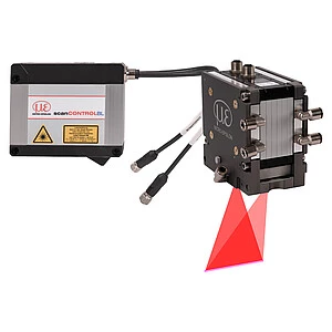
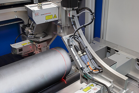
Laser profile scanners from Micro-Epsilon are used to inspect the geometry of silicon ingots. These detect the complete geometry of the silicon rods. This allows geometrical deviations of the silicon block to be determined before separation.…
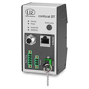
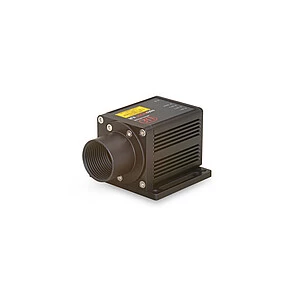
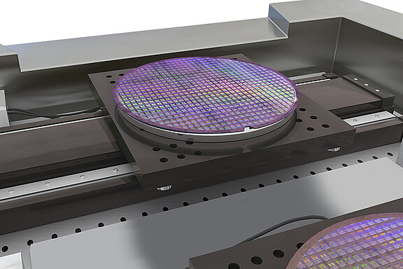
Confocal chromatic sensors scan the wafer surface to detect bow, warp and distortion. Providing high measuring rate, confocalDT controllers enable highly dynamic measurements, allowing the wafer to be inspected within short cycle times. …
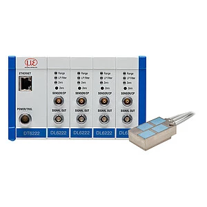
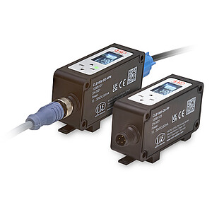
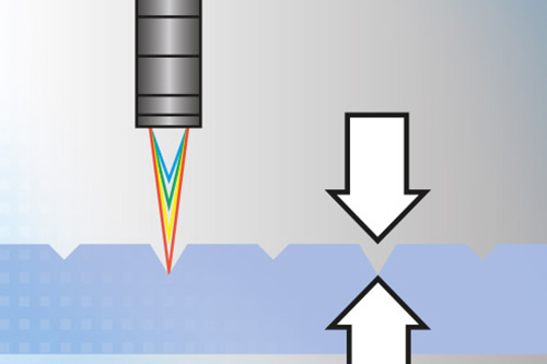
For automatic detection and measurement of saw marks, confocal chromatic sensors from Micro-Epsilon are used. The fast surface compensation feature of the controller regulates the exposure cycles in order to achieve maximum signal stability on…
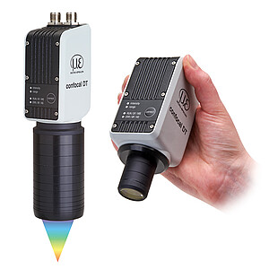
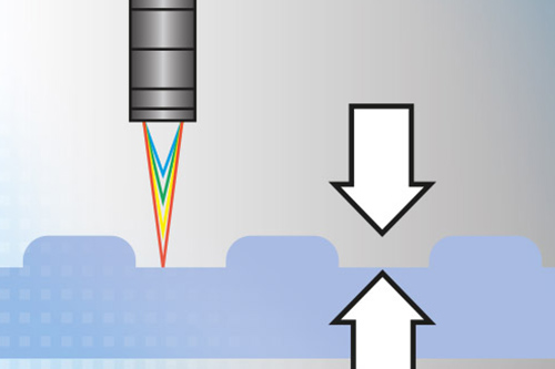
Confocal chromatic displacement sensors from Micro-Epsilon are used to inspect bumps. They generate a small light spot onto the wafer, while reliably detecting the smallest of parts and structures at high resolutions. Therefore, shape and…
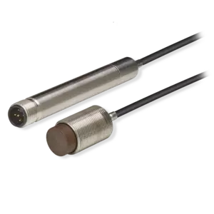
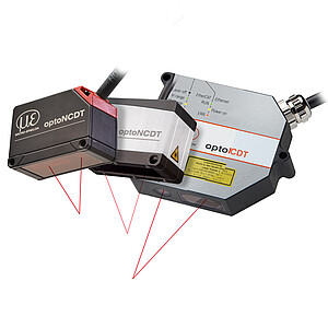
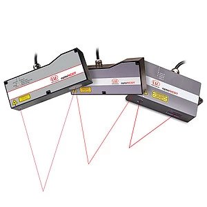
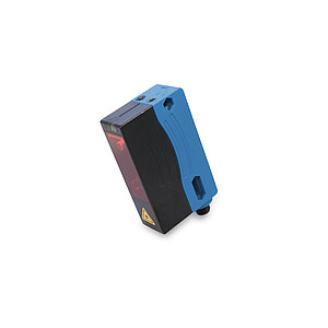
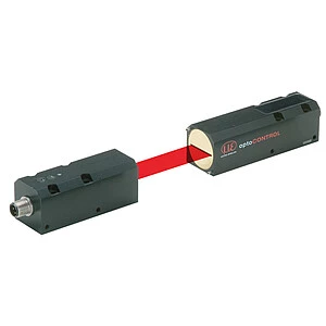
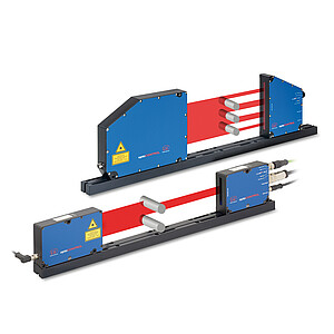
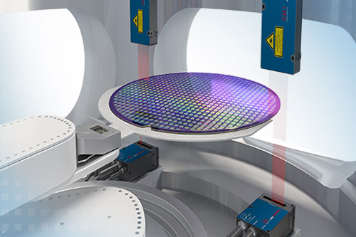
When handling wafers, exact and repeatable positioning is crucial. During the infeed of wafers, two optoCONTROL laser micrometers inspect the diameter and thus determine the horizontal position. Thanks to the high measuring rate and accuracy,…
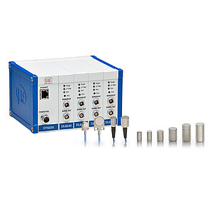
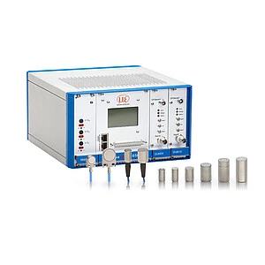
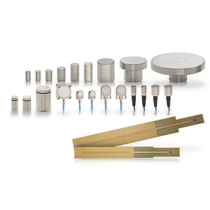
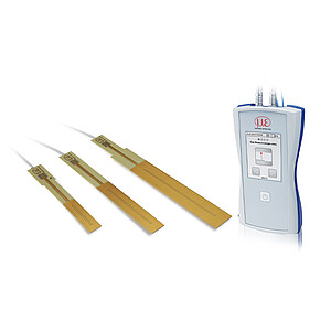
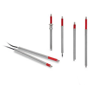
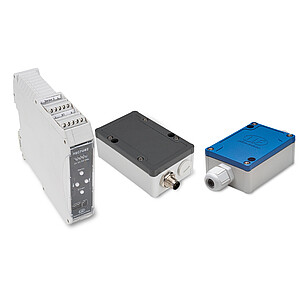
Lithography processes require high resolution and long-term measurement of machine movements in order to achieve maximum precision. High resolutions enable nanometer-precise positioning of masks using capacitive sensors from Micro-Epsilon. Their…
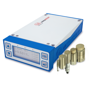
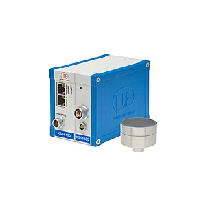
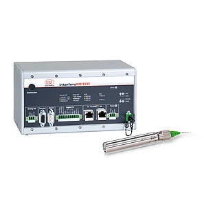
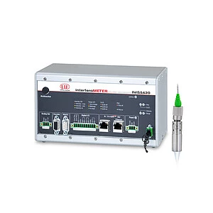
Lithography processes require high resolution and long-term stable measurement of machine movements in order to achieve maximum precision. Thanks to special evaluation algorithms and active temperature compensation, the IMS5400 white light…
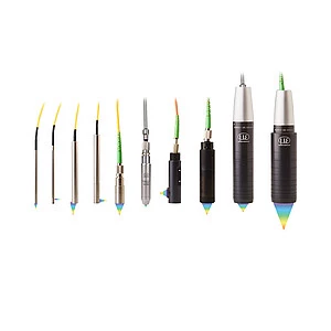
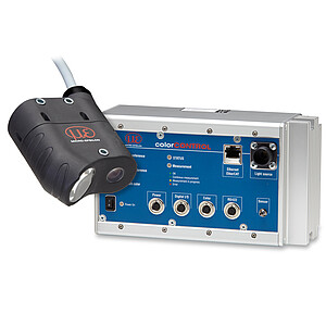
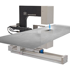
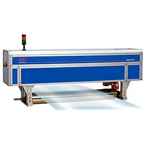
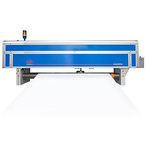
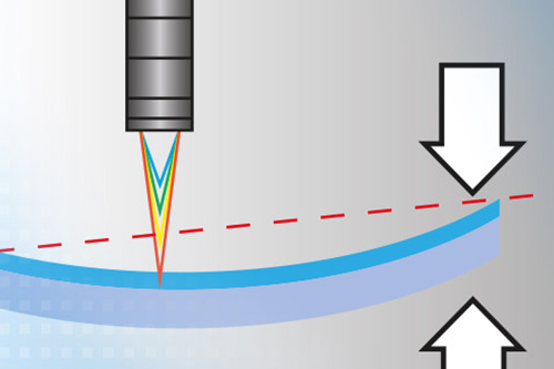
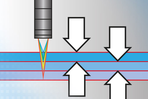
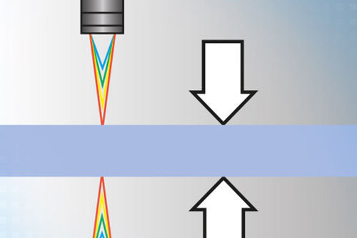
Confocal chromatic sensors are used for one-sided layer thickness measurements. The confocal measuring principle enables the evaluation of several signal peaks, allowing the thickness of transparent materials to be determined. With the multi-peak…
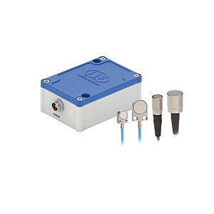
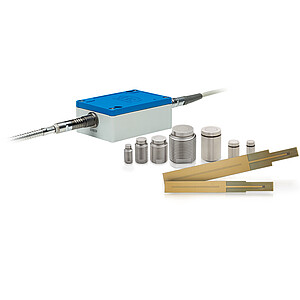
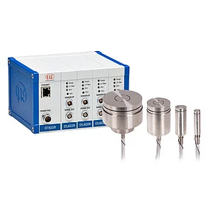
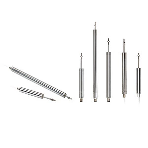
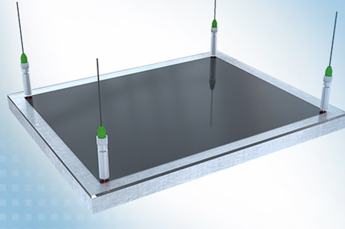
Capacitive displacement sensors are used for fine positioning tasks in the wafer stage. These sensors measure the position of the stage at various points, which is particularly useful for fine alignment. Thanks to their triaxial design, the…
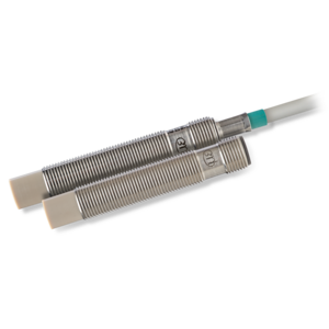
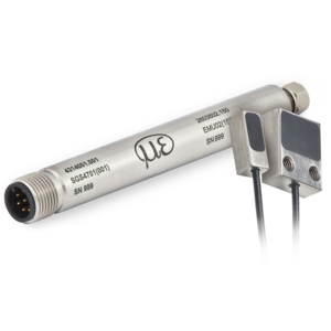
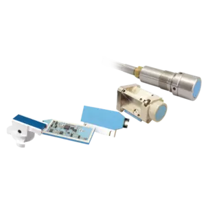
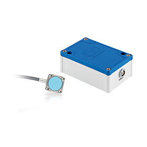
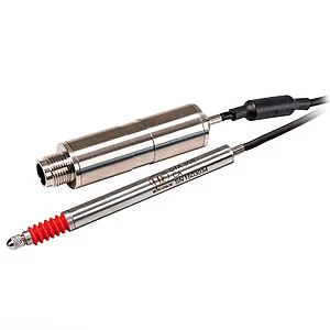
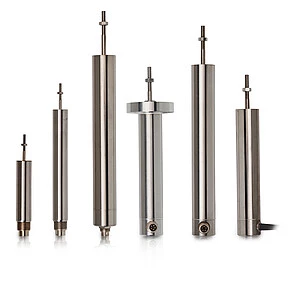
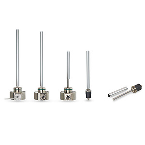
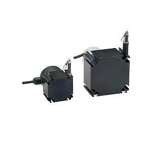
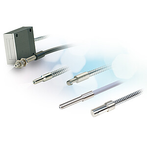
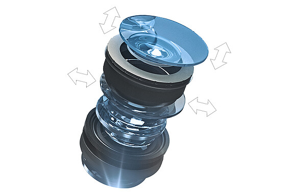
Non-contact, inductive displacement sensors (eddy current) measure the position of lens elements in order to achieve the highest possible imaging accuracy. Depending on the lens system, displacement sensors from Micro-Epsilon are used to detect…
To illuminate individual components on the wafer, the lithographic devices move the wafer to the respective position. Capacitive displacement sensors measure the position of the travel path in order to enable nanometer-accurate positioning. …
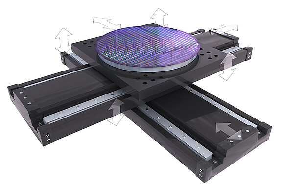
Non-contact sensors from Micro-Epsilon are used for position monitoring of the wafer stage, where they measure highly dynamic XYZ movements of the stage which accelerates very rapidly. Capacitive and inductive (eddy current) sensors achieve…
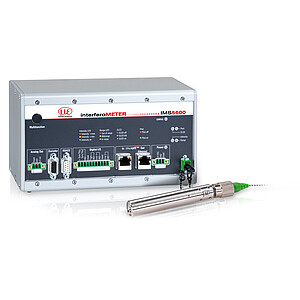
The white light interferoMETER IMS5600 from Micro-Epsilon is used for position monitoring of the wafer stage. It measures the XYZ movements of the stage with extremely high accelerations. The high-precision optical measuring system achieves a…
Capacitive displacement sensors measure the tilt angle of lens carriers to nanometer accuracy. Thanks to the high-precision measurement, a repeatable projection is ensured. Several sensors measure onto the metallic carrier. Their extremely high…
Confocal chromatic sensors are used to measure the alignment of the lens. Several sensors measure directly on the lens to detect the tilt angle to nanometer accuracy. Unlike electromagnetic sensors, confocal chromatic sensors measure reliably…
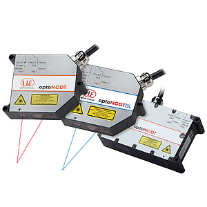
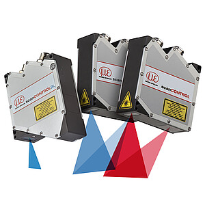
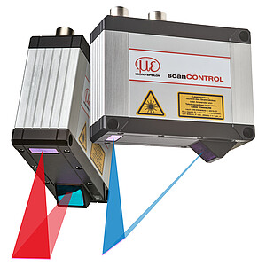
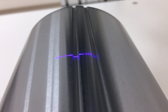
Ingots are often provided with orientation notches, which are necessary for the alignment of the ingots. Blue laser scanners from Micro-Epsilon are used to inspect the profile of the notches for dimensional accuracy. They detect the notch profile…
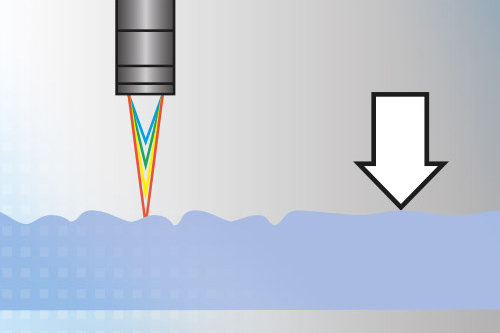
Confocal chromatic sensors from Micro-Epsilon are used to detect cracks and other defects on the wafer. They reliably detect surfaces with varying reflection characteristics due to a fast surface compensation feature. An extremely small light…
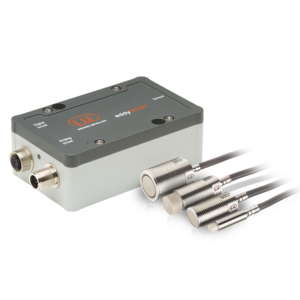
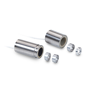
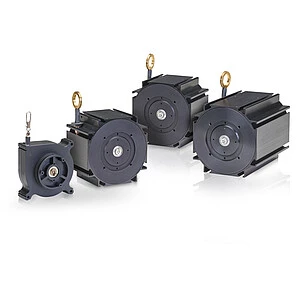
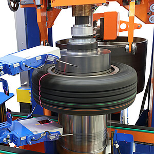
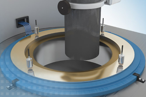
Annular saws are used for cutting silicon ingots. In order to achieve reliable separation of the ingot, the saw blade or holder is monitored using eddy current sensors. Four sensors measure the distance to the support of the saw without contact.…
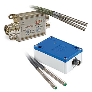
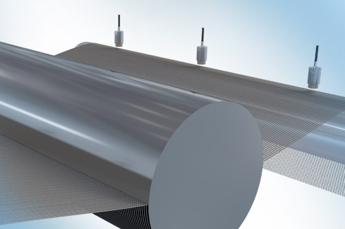
Wire saws are used to cut ingots in only one step. Since the wire is subject to strong wear, the wire bed is monitored at several points using non-contact eddy current sensors. These not only detect the wire height on the guide roller but also…
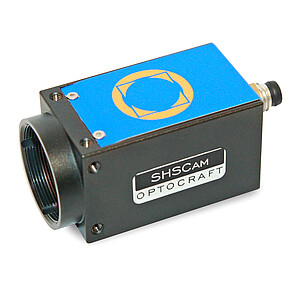
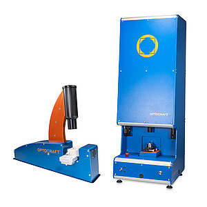
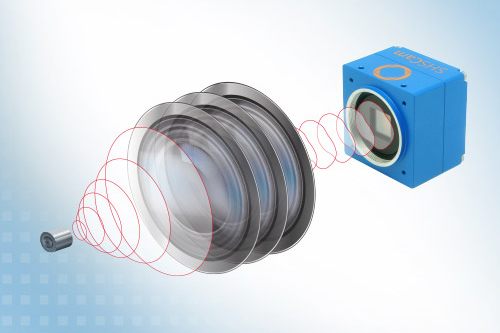
Shack-Hartmann wavefront sensors from Optocraft measure the alignment state and the imaging quality of the entire optical system. The robust measuring principle allows machine integration and automated measuring sequences, as well as laser beam…
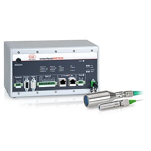
The exact position of the wafer plays an important role in wafer handling. During the infeed of wafers, white light interferometers measure the horizontal tilt angle of wafers. Two interferometers measure onto the wafer. White light…
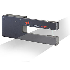
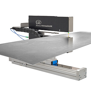
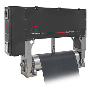
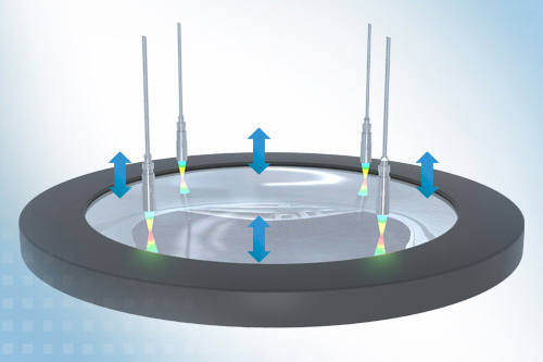
Confocal chromatic sensors measure the thickness deviation (Total Thickness Variation) and the wafer thickness from both sides. Based on the wafer thickness profile, bow and warp of the wafer can be detected. High measuring rates enable thickness…